

IFSC/USPLaboratory in the IFSC: minute structures for use in electronics and medicineIFSC/USP
The use of lasers in medicine – in eye surgery, for example – and in telecommunications, inside optical fibers, is already well known. However, the various types of laser can also be exploited in other activities. Currently, these beams of concentrated light are employed in scientific and technological research to look for a broader use for them on micrometric and nanometric scales. An important step toward this was taken by researchers from the São Carlos Institute of Physics of the University of São Paulo (IFSC/USP). In partnership with a group of researchers from Harvard University in the United States, they have mastered the optical technique that uses ultra-short laser light pulses to produce three-dimensional, complex geometry polymeric structures invisible to the naked eye. Mastery of this new process will, in the future, enable the manufacturing of miniaturized devices for electrical circuits, microcapsules for controlled release of medication, micro-needles for medical use, micrometric or nanometric optical memories, micro-platforms for growing biological tissue, wave microguides for telecom devices, and minute elements for information processing systems, such as the as of yet unprecedented optical computers.
Called two-photon absorption photopolymerization, the technique is very new and was proposed in 1997 by the Japanese researcher Satoshi Kawata, a professor who specializes in nanotechnology at the University of Osaka. It was not until 2001, when Kawata’s group published an article in the journal, Nature, that he became known in international scientific circles. Currently, there are just a few research groups in the world, notably in Japan, the United States, Germany and South Korea, which have managed to reproduce photopolymerization. Thanks to the group from São Carlos, this set of countries now includes Brazil.
To size up the advance that this technique represents, one must first be aware that that polymerization is a chemical reaction that produces a wide range of plastics. By means of this process, molecules called monomers are chemically bonded, resulting in solid materials consisting of macromolecules. The polymerization reaction can be triggered in many ways, one of which is optically, through exposure to light, when the reaction is called photopolymerization. In this case, a compound called a photoinitiator is used; when this absorbs the light that falls on it, it kicks off the process of transforming the sticky, liquid resin into a solid. The main distinguishing feature of two-photon absorption photopolymerization is that the reaction is confined to the region on which the light is focused, meaning that the material only solidifies at this point. By moving the laser beam and, therefore, its focus, one can produce complex three-dimensional structures with resolution that is micrometric and nanometric, i.e., whose scale is measured thousandths or millionths of a millimeter.
“To put it more simply, we can say that as the computer-controlled laser beam runs over the polymeric resin, the material hardens. It’s as if the laser beam draws by solidification the desired structure in three-dimensional space, and not just on a flat surface,” says physicist Cleber Mendonça, a professor from IFSC and leader of the study. “In traditional photopolymerization, where just one photon is absorbed by the photoinitiator compound, it’s impossible to produce such small three-dimensional structures,” the researcher points out, emphasizing that the new technique depends on high light intensity, generated by lasers pulsating in femtoseconds, a unit of time equal to one quadrillionth of a second, or 10-15 seconds. Currently, femtosecond laser pulses are used in research aimed mainly at developing optical transistors.
The partnership with Harvard University, which allowed this technique to be mastered, started in August 2005 when Cleber Mendonça was doing his postdoctorate, which he finished in December 2007, with Professor Eric Mazur’s group, in the Physics Department and School of Engineering and Applied Sciences of that university. Mazur is considered one of the world’s leading authorities in the use of ultra-short laser pulses for micro-manufacturing and micro-structuring materials. His research abroad had the support of a FAPESP grant of the New Frontiers type, which is for funding long-stay training programs in international centers of excellence in research areas in which the State of São Paulo is still deficient. “For some years the Photonics Group of the São Carlos Institute of Physics had been working with non-linear optical processes – which depend on the intensity of light – and with ultra-short laser light pulses. However, it was while at Harvard that I had contact with the two-photon absorption photopolymerization technique,” says Mendonça, who also has FAPESP funding via a regular research aid project. In this project, the researcher is also investigating the use of femtosecond lasers in (two-dimensional) surface structuring of materials.
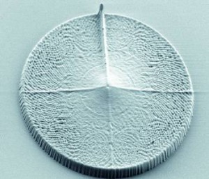
IFSC/USPElectronic microscopy of different structures produced with laser beams and polymersIFSC/USP
Although it is a fairly promising technique in the micro-manufacturing area, Mendonça says that there are still no products commercially produced with this process, just prototypes. “We believe that in a few years the first commercial micro-structures made with this two-photon absorption photopolymerization process should be on the market. The most advanced studies are concentrating on the MEMS area – micro-electro-mechanical systems on a micrometric scale – for such things as sensors, motors and actuators,” says the researcher from USP. One of the pioneers in the new technique is Focal Point Microsystems LLC, and American enterprise that is a spin-off from research conducted at the Georgia Institute of Technology, better known as Georgia Tech, in the United States. The firm was founded by researchers from this institution and is developing a commercial workbench for two-photon absorption photopolymerization for use in commercial MEMS applications.
Doped compounds
A major distinguishing feature of the work being done in São Carlos is the doping of polymeric microstructures with organic compounds. Doping is the scientific term used to indicate the addition of foreign substances to any material for specific, well-defined purposes, such as improving some of its mechanical properties, for example. Doping enables the production of micro or nanoelements with optical, electrical or biologically active features suitable for certain applications. “In our work we’ve already doped base-resins with organic colorants and with electroluminescent and biocompatible polymers. In all three cases doping is carried out prior to the laser manufacturing process,” says Mendonça. According to the researcher, the doping technique in itself is widely used by research groups all over the world, but resin doping used in manufacturing micro and nanostructures by means of the two-photon absorption photopolymerization process is something extremely new.
The focus of one of these studies was the area of engineering systems for growing biological tissue, such as bone, cartilage and skin. An important step in this research, which may lead to advances in the production of human prostheses, is understanding cell movement and adhesion. The study of this phenomenon in a laboratory depends on the availability of micro or nanometric matrixes where the cells can move and to which they can adhere. That is where two-photon absorption photopolymerization comes in. “Thanks to this technique we develop purpose-designed 3D structures that enable systematic investigation of cell adhesion and migration. This research may facilitate the development of new techniques in tissue engineering because it enables one to study cell behavior better,” states Mendonça. Some years ago, a group of Finnish researchers from the University of Tampere, in Finland, announced advances in the development of structures for use as support for the growth of living tissue.
Other work of the USP Photonics Group, whose results were published in this year’s September issue of Applied Physics Letters, concentrated on the development of microstructures containing organic light-emitting compounds with special optical properties. These devices can be used in the production of optical circuits or optical sensors. In this case, the miniaturized light source is included in the device and directly attached to the other elements that comprise the optical circuit. The group also expects to produce structures containing organic molecules that, in the presence of a luminous excitation source, become oriented in a given direction. “This orientation could be used as a means of storing information. Areas where the molecules are oriented in a given direction would correspond to the presence of information, whereas areas where they are randomly distributed would correspond to the absence of data, in a process akin to what happens with CDs or the HDs in our computers,” points out Mendonça.
According to the researcher, all these advances in photonics are due to some extent to the choice of polymeric resins as the basic material to work with. The advantage of using these resins rather than other materials such as porcelain, glass or metal, is that they enable carrying out the reaction at room temperature and ambient pressure. With other types of materials, this would be impossible. “They would have to be used in powder-form for the particles to join by a process of diffusion as a result of exposure to the light,” he says. In these cases, however, there would be less control over the manufacturing process. “Furthermore, polymeric materials are easier to dope and the properties of end products made from them, such as flexibility, optical transparency and the refraction index are entirely different from the properties of products made from ceramics and metals.”
The projects
1. Ultrafast dynamics and determination of the dielectric function in organic materials (nº 05/50621-5); Type Grant for Research Abroad – New Frontiers; Coordinator Cleber Renato Mendonça – USP; Investment R$ 61,633.61 (FAPESP)
2. Micro-manufacturing and microstructuring in polymeric materials using a femtosecond laser (nº 08/00652-0); Type Regular Research Awards; Coordinator Cleber Renato Mendonça – USP; Investment US$ 87,731.25 and R$ 3,450.00 (FAPESP)
Scientific articles
MENDONÇA, C.R. et al. Three-dimensional fabrication of optically active microstructures containing an electroluminescent polymer. Applied Physics Letters. v. 95, p. 11.330-9. 2009.
CORREA, D.S. et al. Two-photon polymerization for fabricating structures containing the biopolymer chitosan. Journal of Nanoscience and Nanotechnology. v. 9, p. 5.845-9. 2009.