
MARCELO GOUVEIA/ LAFE-UNICAMPOptic filter: ring made from a microfiber with a 3-micron diameterMARCELO GOUVEIA/ LAFE-UNICAMP
Information technology tends toward constant miniaturization. This evolution includes, among other elements, totally optic circuits in which chips can communicate with the light waves of lasers. Future connections could include optic microfibers and nanofibers that would be far superior to the electrons found on the current circuit boards of computers. These devices have been studied since 2009 at the Special Fibers Laboratory (LaFE) of the Gleb Wataghin Physics Institute (IFGW) of the State University of Campinas (Unicamp).
The earliest results have already materialized and are part of nanophotonics, a new field that encompasses the transmission of information through light waves in microscopic-sized equipment that is much smaller than the current devices. “This is communication from light to light in which nanometric circuits process and transmit data,” says professor Cristiano Monteiro de Barros Cordeiro, coordinator of LaFE. The laboratory is part of the Research Center on Optics and Photonics of Campinas, funded by FAPESP under the Research, Innovation and Diffusion Centers (Cepid) program, coordinated by professor Hugo Fragnito.
At IFGW, which is also part of the National Institute of Science and Technology of Optic Communication Photonics (Fotonicom), the researchers are studying devices that are approximately 10 centimeters long, with a diameter ranging from 10 microns (1 micron is one thousandth of 1 millimeter) to 200 nanometers (1 nanometer is equal to 1 millimeter divided by 1 million). Their size is 500 times smaller than the diameter of a hair strand. The commercial fibers installed in big cities and underwater cables, for example, that are used to run the internet and the telephone systems, have internal diameters of 8 microns, through which the light travels, and a silica shell (also called glass) with a diameter of 125 microns. These cables are many kilometers long.

CLAUDECIR BIAZOLI/LAFE-UNICAMPEquipment used to produce microfibers and nanofibers at UnicampCLAUDECIR BIAZOLI/LAFE-UNICAMP
The operational advantages of these fibers include less energy consumption, less heating of the system, and higher data transmission capacity than that of existing electronic circuit boards. Another feature of these tiny fibers is their thinness and flexibility; this makes it possible to integrate a full optic system inside the computer. The outstanding feature is that some of the fibers with a diameter of less than 1 micron are shorter than the length of the wave of typical 1.5 micron laser beams used for optic communications. Thus, part of the light remains outside the fiber wall, but the light wave continues lengthwise along the device. The light follows the fiber when it is swung from side to side. “Whether part of this light that remains can help or hinder the future optic interconnection is still an unanswered question in all the groups around the world that study these fibers,” says professor Cristiano. These groups include the United Kingdom’s University of Southampton, and the company OFS Laboratories, linked to the Furukawa Corporation.
These micro and nanofibers are also being studied with the prospect of using them in sensors, for gas detection, and for chemical and biological sensing. An example would be detecting water polluted by the Escherichia coli bacteria. “There is a possibility that these fibers could be given the function of detecting the bacteria by means of alterations in the transmission of the light and the resulting identification of the microorganism,” says Cristiano. His team conducted an experiment at the lab of IFGW that entailed manipulating bacteria and yeasts in a liquid medium. They were able to select or park a group of bacteria on a microfiber with a diameter of 500 nanometers. This kind of experiment could be useful for studies on the antibodies of this kind of microorganism.
Another sensor-related functionality of these fibers has led to filing a patent request with the National Institute of Industrial Property (INPI) at the end of 2011. The group was able to produce a fiber 50 times more sensitive to mechanical traction than the fibers made for civil construction. These fibers are fastened along structures, such as bridges, and are used to measure, through changes in the light, structural deformations caused by a truck being driven over the bridge, for example.
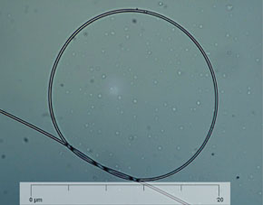
Still in the field of optic communications, the researchers created a ring-shaped optic fiber from a fiber with a diameter of 3 microns that only lets through one wave length. The laboratory production of these devices with specific features uses heating and pulling (similar to the stretching of commercial fibers). “It is similar to heating up a fishing line and pulling it until it achieves the nanometric thickness,” Cristiano explains.
The Project
1. Center for Research on Optics and Photonics of Campinas (CePOF) – (nº 2005/51689-2); Modality Centers of Research, Innovation and Dissemination (Cepid); Coordinator Hugo Fragnito – Unicamp; Investment R$ 1 million a year for the entire CePOF (FAPESP)
2. Photonics for optic communications – INCT (nº 2008/57857-2); Modality Thematic Project; Coordinator Hugo Fragnito – Unicamp; Investment R$ 1,021,698.99 and US$ 1,027,935.95 (FAPESP and CNPq)