A new generation of optical lenses is being developed and tested at multiple universities and companies worldwide. These lenses, known as metalenses, are silicon films a thousand times thinner than a sheet of paper. They perform the same functions as conventional glass or plastic lenses but are able to focus light with far greater precision. As these technologies advance, metalenses — also known as optical metasurfaces — may soon replace the traditional lenses used in cell phone cameras, microscopes, endoscopes (medical devices used for visualizing the interior of hollow organs), virtual reality goggles, and telescope systems.
Emiliano Rezende Martins and Ben-Hur Viana Borges, both electrical engineers from the University of São Paulo at São Carlos School of Engineering (EESC-USP), are developing metalens prototypes combining multiple optical features in a single lens, such as wide angle and high focusing efficiency — two properties currently achievable only with multiple glass or plastic lenses.
Martins recognizes that a number of hurdles need to be overcome to develop commercially functional metalenses. Among the primary hurdles is making metalenses larger than a few hundred micrometers (1 micrometer equates to one-thousandth of a millimeter) in diameter and that can focus multiple colors without creating image distortions — a phenomenon referred to as chromatic aberration. In conventional curved lenses, chromatic aberration can be resolved by stacking multiple lenses together, a technique commonly seen in smart phone cameras.
In collaboration with Chinese researchers, the São Carlos group is developing a red-green-blue (RGB) metalens prototype that could provide an alternative solution in digital-imaging systems. The device was designed with the assistance of the Brazilian researchers and then fabricated in China due to equipment constraints.
A fundamental property of lenses is their numerical aperture, or the ratio of the radius of the light-capturing area to the focal length. The larger the aperture the higher the lens resolution. For a lens immersed in air, the highest possible numerical aperture is 1. One of the major challenges within the field of metalenses is achieving large apertures for large-diameter lenses. The São Carlos group’s prototype has a numerical aperture of 0.8 with a lens thickness of 1.8 micrometers (roughly 50 times smaller than the diameter of a strand of hair) and a diameter of 1 millimeter (mm) —“10 times larger than the prototypes developed by other researchers,” notes Martins, one of the authors of a paper published in NanoLetters in May 2022.
This was achieved through two innovations developed by the group. The first is a dual-layer structure instead of the three layers used by other researchers, which simplifies the fabrication process to some extent. The structure is made with layers of different materials and thicknesses designed to facilitate the passage of light — an upper layer of silicon nitride, measuring 600 nanometers (nm; 1 nanometer is equivalent to one billionth of a meter), and a lower layer of crystalline silicon, measuring 400 nm.
The second innovation involved the incorporation of nanoposts of different shapes — square and circular — rather than a single shape. Nanoposts are tiny structures that modulate the passage of light, visible only under a scanning electron microscope. The nanoposts positioned closest to the center of the metalens delay the light beam, synchronizing its arrival at the focal point with the light originating from the peripheral region, which travels a longer distance.
Martins offers a comparison: “Think of the metalens as a highway. The light passing through it is comparable to cars moving at different speeds. The nanoposts act as barriers, momentarily slowing down the faster light waves before releasing them, ensuring that they all arrive at the desired destination at the same time.”
This operates on the same principle as conventional lenses, which, by virtue of their material and curvature, are able to guide light rays originating from various parts of the lens to converge at a single point and create the image’s focal point. The nanoposts are able to precisely control the passage of light due to their dimensions being equal to or even smaller than the wavelengths of light waves. Depending on the application, they can also be used to alter the wave properties in different ways. “We have also increased the number of nanoposts to synchronize wave delay for the three different colors,” Martins explains.
Since the layers of metalenses are typically etched onto silicon surfaces using a technique known as electron beam lithography, stacking multiple layers demands a high degree of precision and is difficult to automate, says Martins. A simpler approach is to create metalenses with just one layer, a possibility currently feasible only for single-color lenses.
“The São Carlos group got promising results for all three color bands, covering virtually the entire visible light spectrum, across a relatively large area compared to previous lenses,” says electrical engineer Hugo Enrique Hernández Figueroa from the University of Campinas (UNICAMP), who was not involved in the study.
In a separate project, the São Carlos group designed a prototype monochromatic metalens with a single silicon layer. This lens is capable of producing high-resolution images but only in the green color spectrum, offering either a limited field of view or, conversely, reduced resolution with a wide angle.
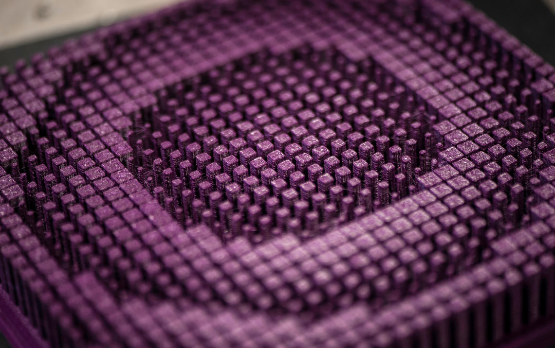
Léo Ramos Chaves / Revista Pesquisa FAPESPA plastic metalens measuring 20 cm in diameter was used to study the effect of nanoposts (shown in lilac) on electromagnetic wavesLéo Ramos Chaves / Revista Pesquisa FAPESP
“Metalenses are uniquely able to combine two or more functions due to their precise control over light properties,” explains electrical engineer Augusto Martins, the lead author of a March 2022 article in Advanced Optical Materials. As part of his doctoral studies, which he concluded in 2021 at EESC-USP, Martins spent time at the University of York in the UK, where he built a prototype metalens. His thesis earned him the 2022 Capes Award in Engineering IV.
The original elliptical design of the nanoposts enabled the metalens to alternate between offering a wider angle or achieving superior focus and resolution. This was achieved by using a different filter (or polarizer) for each effect. One potential application for his metalens could be in endoscopy, where a metalens-equipped device could be finely tuned to capture intricate details within the subject organism. Rezende Martins, one of the authors, believes these devices could be made significantly smaller than current counterparts if they could use a single metalens film.
Metalenses are being designed for larger devices as well. In an article in the December 2022 issue of NanoLetters, researchers from the University of Pennsylvania presented a monochromatic image of the lunar surface obtained using a prototype ultra-thin, 8 cm diameter telescope objective that focuses a single wavelength — infrared light.
“Demand for single-color metalenses, such as those utilized for 3D environmental detection in applications like facial recognition cameras or autonomous vehicles, is expected to outpace demand for multi-color lenses, like those used on smart phones,” says Augusto Martins. “Single-layer metalenses could be manufactured using the same manufacturing processes as for electronic devices, allowing for easier integration into electronic appliances,” Rezende Martins adds.
“Metalenses represent an evolution from conventional lenses,” notes physicist Jarbas Caiado de Castro Neto from the Institute of Physics in São Carlos (IFSC) at USP, who was not involved in the EESC studies. “As research in this field progresses, one of the major advantages will be a significant reduction in the production costs of electronic devices, as multiple lenses could be replaced by a single film.” Castro Neto is one of the founding partners of Opto Eletrônica, a company in São Carlos that develops optical components and instruments for the medical, industrial, and aerospace sectors.
Facial recognition projectors
Founded by Italian-American physicist Federico Capasso at Harvard University, a leading expert in optical metasurfaces, the Boston-based startup Metalenz unveiled in May 2021 on its website a new range of projectors designed for facial recognition in smartphones and other applications.
In these projectors, a single metalens replaces as many as six optical components, including four conventional refractive lenses that align emitted infrared light for facial recognition. “What Capasso’s company has developed is an extreme illustration of the capabilities of metalenses: integrating multiple optical elements into a single film,” says Martin.
In September 2022, Metalenz announced a partnership with STMicroeletronics — a semiconductor manufacturer based in Geneva, Switzerland — to manufacture sensor systems for facial recognition in smartphones. The metalenses will be made with silicon discs and other electronic components, all in a single production line.
Projects
1. Metasurfaces for imaging and sensing (nº 20/00619-4); Grant Mechanism Regular Research Grant; Principal Investigator Emiliano Rezende Martins; Investment R$69,209.35.
2. Strongly resonant all-dielectric metasurfaces based on near-dark and toroidal modes (nº 21/06506-0); Principal Investigator Hugo Enrique Hernández Figueroa; Investment R$246,276.88.
Scientific articles
FENG, W. et al. RGB achromatic metalens doublet for digital imaging. NanoLetters. vol. 22, no. 10, pp. 3969–75. may 4, 2022.
MARTINS, A. et al. Correction of aberrations via polarization in single layer metalenses. Advanced Optical Materials. vol. 10, no. 2102555. mar. 10, 2022.
ZHANG, L. et al. High-efficiency, 80 mm aperture metalens telescope. NanoLetters. vol. 23, no. 1, pp. 51–7. dec. 16, 2022.
Republish

