Léo RamosRepresentation of electrons with aligned spinsLéo Ramos
Over the last three years, something akin to a fever has spread like wildfire throughout the sub-area of physics that studies solids, the so-called physics of condensed matter. The current mania concerns a new class of materials with unique electronic properties, which have been given the somewhat intimidating name of topological insulating materials. “They are fantastic,” states the physicist Adalberto Fazzio, from the University of São Paulo (USP), who is a coordinator for the Ministry of Science and Technology’s nanotechnology division.
Fazzio witnessed the explosion of interest in topological insulating materials during the March 2010 meeting of the American Physical Society, when researchers from all over the world crowded together to attend the lectures about the first conclusive evidence of the relatively cheap production of these materials. The only reason why studies of topological insulating materials have not become more widespread since then is the complex theory that underlies them and the sophisticated techniques required to analyze these materials in laboratories – challenges that have recently been taken up by two Brazilian groups: a theoretical one, headed up by Fazzio, and an experimental one, coordinated by the physicist Vagner Eustáquio de Carvalho, from the Federal University of Minas Gerais (UFMG).
According to Carvalho, the hope that this new favorite of condensed matter is more than just a passing fad remains high. “The possibilities in terms of technological applications are real,” He says. “I have no doubt whatsoever that within another five years electronic devices will be produced based on these materials.”
The secret of the success of these topological insulating materials is their surface. In papers published between 2005 and 2006, two US teams of theoretical physicists, one led by Charles Kane, from the University of Pennsylvania, and the other by Joel Moore, from the University of California at Berkeley, predicted that negatively charged particles, electrons, would behave very strangely if they passed through a piece of crystal made from certain heavy metals, such as bismuth. The electrons would avoid the inner part of the material, only spreading along the surface of the crystal. There was nothing amazing in this per se. The crystal would work like the inside of an electric wire, with the insulating core enveloped by an electricity conducting metallic outer layer.
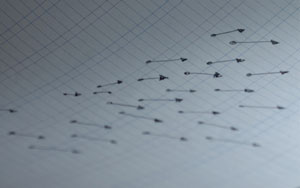
 Igor ZolnerkevicWhat caused the physicists’ jaws to drop was the orderly way in which the electrons spontaneously seemed to move around the surface. Electrons have a magnetic property called spin, which can be represented as a small arrow. Just as the spins of the electrons in a magnet all point in the same direction, giving the material its magnetic properties, the electrons of an electric current sliding across the surface of a topological insulating material have their spins aligned, like a perfectly-straight row of soldiers with their bayonets all pointing in the same direction. This sort of behavior had only ever been seen before in materials subject to very strong magnetic fields and at extremely low temperatures, close to absolute zero, while in the case of the topological insulating material, they did this by themselves, without any need to apply external fields, and at environmental temperatures.
Additionally, this fierce inclination to order means that the electrons rapidly pass over any small imperfections or impurities on the surface of the crystal, without deviating or losing energy as they do in the case of most materials. These high speed, organized currents allowed the engineers to inaugurate the era of spintronics. The idea is to use electron spin not just to construct the current tiny magnetic memories, but also new magnetic transistors, which would process information more quickly and in an energy-efficient way, in the form of zeros and ones encoded in the spin. There are also theoretical papers showing that in principle it would be possible to use the collective behavior of the electrons in the topological insulating material to undertake a new type of computing, namely, quantum computing, which would be exponentially faster than conventional computing.
The origin of the topological insulating materials lies in the interaction between the spin and the orbit of the electrons, a phenomenon that occurs in atoms with a high atomic number and that physicists call the spin-orbit interaction. According to the theory, this interaction alters an abstract property of the mathematical functions that describe the movement of the electrons. It is the inversion of this property that is known as parity, which creates the special states of electrical conduction on the surface of the material. Without a sufficiently strong spin-orbit interaction, the material would work just like a normal insulating material.
 Igor ZolnerkevicTo better understand the origin and the properties of surface states, Fazzio and his PhD students at USP, Leonardo Abdalla and Leandro Rocha, along with Tomé Schmidt and Roberto Miwa, both of whom are physicists at the Federal University of Uberlândia, in the State of Minas Gerais, solved the quantum mechanics equations including the spin-orbit interaction, with the help of computers, describing the atom-by-atom structure of one of the topological insulating materials that has been highly studied in laboratories: bismuth selenide (Bi2Se3).
The crystal is formed by the stacking of compact blocs consisting of three atomic layers of selenium interspersed with two of bismuth. Between these 5-atom thick blocs, there is a larger space, known as the Van der Waals gap, where the interatomic connections are weaker. In one of the computer simulations, the result of which has not yet been published, the researchers forced the separation between these two blocs. Thus, they managed to observe, step by step, the birth of the conduction states in the surfaces created by the variation of this gap in the crystal, checking what the minimum space should be in order for them to appear – in this case, 7.2 angstroms.
In another study, to be presented on the 28th of this month at a meeting of the American Physical Society, in Boston, Fazzio, Schmidt and Miwa used the same computational techniques to investigate what would happen with the bismuth selenide if it were exposed to the air and a few oxygen atoms were to take up residence in the crystal. The simulation that they carried out showed that, unlike materials such as silicon, in which oxidization can completely destroy its electronic properties, bismuth selenide continues to be a topological insulating material in the presence of oxygen. Oxidization merely increases the energy of the conductive states slightly, an effect that may be exploited in order to control these states in future technological applications.

ALI YAZDANI / PRINCETON UNIVERSITY / SCIENCE PHOTO LIBRARY/LATINSTOCKElectrons spread on surfaces with defects in the topological insulating materialALI YAZDANI / PRINCETON UNIVERSITY / SCIENCE PHOTO LIBRARY/LATINSTOCK
Meanwhile, in another study that was published in December 2011, in the scientific journal Physical Review B, the trio of theoretical physicists simulated inserting cobalt atoms in bismuth selenide. Unlike what happened with oxygen, the magnetic properties of cobalt cause this atom to interfere in the spin-orbit interaction, destroying the “protection” of the surface conductive states against impurities and defects in the crystal. However, the cobalt atoms generate among themselves a new orderly standard of spins. Whereas in the pure material the spins of the electrons are aligned in parallel with the surface of the material, the presence of cobalt introduces new states, aligned at right angles to the surface. These right angled spin-states could be used to encode magnetic memories in future atomic scale devices.
Search for the ideal
However, to carry out all these technological applications, there are still a number of obstacles that must be overcome. The main one is that the samples of bismuth selenide and of another promising material, bismuth tellurite (Bi2Te3), analyzed so far have only roughly behaved like topological insulating materials. Inevitable impurities cause their interior to conduct a little electricity. This residual current can interfere in the orderly spin current on the surface. “Achieving completely clean surface states is fundamental for any technological application of these materials,” explains Carvalho.
The group of researchers from UFMG were lucky. When interest in topological insulating materials rocketed, Carvalho and his colleagues already had samples of Bi2Te3 and Bi2Se3, ready, which they had produced for a previous project that involved studying the thermoelectric properties of these materials.
A study undertaken in collaboration with the group of physicist Philip Hofmann, from the University of Aarhus, Denmark, which was presented in August 2011 at the Tenth International Conference of Surface Structures, held in Hong Kong, revealed that the samples had the quality that was necessary in order to study the properties of topological insulating materials.
In the meantime, Carvalho, Edmar Soares and the students Diogo Reis and Wendell Simões were the first ones to install the technique known as Arpes (Angle-resolved photoemission spectroscopy) in a Brazilian laboratory. With this technique, particles of light emitted by a special light collide with a sample kept in an ultra-high vacuum environment and extract its electrons. A high resolution spectrometer then measures the properties of these electrons, making it possible to deduce their state in the material. The existence of topological insulating materials was confirmed by means of Arpes.
The researchers from the State of Minas Gerais mastered another technique, the diffraction of low energy electrons (Leed), which enabled them to determine the atomic structure on the surface of the samples. They want to combine Leed and Arpes, in order to investigate the influence of the position of the atoms in the material’s electronic states.
Another promising experiment that the group has been conducting is depositing ultrafine layers of other atoms (antimony, copper, tin or manganese) over the Bi2Te3 and Bi2Se3 crystals. Recent surveys showed that the presence of these ultrafine metallic films reduced the density of electrons being conducted through the interior of the material. “The hope,” explains Carvalho, “is that, as we control the presence of these films, we will manage to produce a real topological insulating material.”
The Project
Simulation and modeling of nanostructures and complex materials (n° 2005/59581-6); Modality Thematic Project; Coordinator Adalberto Fazzio – IF/USP; Investment R$ 607.550,62 (FAPESP)
Scientific article
SCHMIDT, T.M. et al. Spin texture and magnetic anisotropy of Co impurities in Bi2Se3 topological insulators. Physical Review B. v. 84. Dec. 13, 2011.