In two articles published at the same time in the journal Nature in early 2018, a research group led by Spanish physicist Pablo Jarillo-Herrero showed that overlaying two graphene sheets—structures that are one atom thick and resemble a honeycomb made of carbon—and rotating one of them very subtly in relation to the other produces two diametrically opposed effects depending on the electron density of the system. At certain electron densities, the material became an insulator, blocking an electric current. But if as well as misaligning one of the graphene layers at an angle of 1.1 degrees, the team from the Massachusetts Institute of Technology (MIT), USA, also slightly increased the number of electrons, the sheets started to behave like a superconductor, allowing an electric current to flow through it without any resistance from the material.
The experiments were conducted at very low temperatures of -271 degrees Celsius, close to absolute zero, but the signs of superconductivity were enough to heat up a field that emerged as theoretical in the late 2000s and has not previously produced any major laboratory achievements: twistronics, the study of what happens when you rotate one of the sheets in a system consisting of two or more layers of graphene or another two-dimensional material, such as molybdenum sulfide (MoS22) or boron nitride (BN). In mid-February this year, a team coordinated by researchers from the Federal University of Minas Gerais (UFMG) presented an optical device that could be fundamental to understanding how twistronics works.
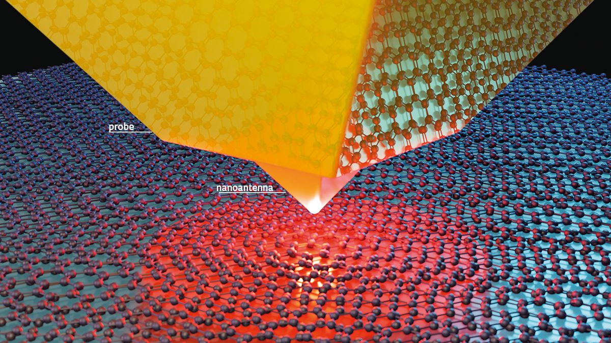
In an article that was featured on the cover of that month’s issue of Nature, the group, led by physicist Ado Jório, described the operation of the nanoscope, a device that produces images on an atomic scale of events occurring inside structures, such as a pair of deliberately misaligned graphene sheets. “With the nanoscope, we can see where the vibrational states of twisted graphene sheets are located and try to understand their local electronic properties,” explains the UFMG researcher. “It is not just a device that produces high resolution images, but a useful tool for understanding twistronics.”
The paper was authored by 13 researchers and graduate students from UFMG, two other Brazilian colleagues—one from the Federal University of Bahia (UFBA) and another from the National Institute of Metrology, Quality, and Technology (INMETRO) in Brasília—and eight coauthors from institutions in Japan, Belgium, and the USA. It presents the results of measurements taken by the nanoscope from two overlapping graphene sheets, one of which was slightly rotated. Like in the experiments by the Jarillo-Herrero’s team at MIT, the slightly misaligned sheet was rotated by various angles around 1.1 degrees, which the academic community calls the magic angle.
Leo Drumond / Nitro
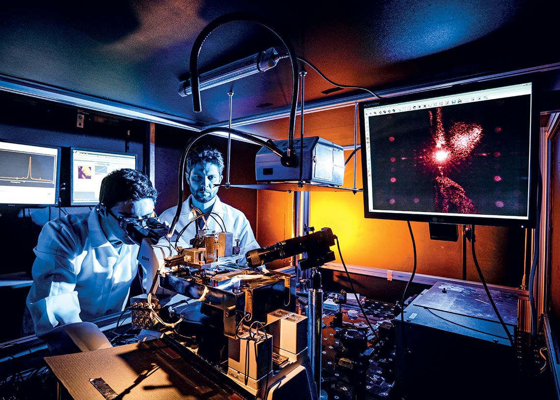
UFMG researchers testing the nanoscopeLeo Drumond / NitroSo far, four nanoscopes have been produced. Two are at UFMG, one at the Federal University of Ceará (UFC), and the fourth is at INMETRO. Two precommercial prototypes are currently being built and should be ready by the middle of the year. With an eye on a possible market for selling the device to research laboratories and companies, nine patents related to the nanoscope were applied for in Brazil, and two abroad. The commercial production rights, which will be shared by UFMG and the entities that funded the research, will probably be transferred to a small company that was started based on the work of Jório’s team and is run by three former students of the UFMG graduate program: Fábrica de Nanosoluções (FabNS).
“When we started in 2018, about 70% of the nanoscope’s components were imported and 30% were produced domestically,” says Cassiano Rabelo, who has a PhD in electrical engineering and was a coauthor of the study and one of the partners of FabNS. “Today, it should probably be the other way around. But the most important thing is our knowledge of how to build the device.” Jório estimates that nanoscopes could be sold for €250,000 (about R$1.6 million) after they have been validated by key customers. “The equipment definitely still needs to be improved and the information generated by first adopters will be very helpful to improve the nanoscope,” says Jório.
The intellectual property for the nanoscope created by UFMG is protected by nine patents
Commercial development of the device began in 2018, but since the mid-2000s, the technological initiative has benefited from investments made by the Brazilian National Council for Scientific and Technological Development (CNPq) in nanotechnology and graphene research carried out by the UFMG group. Funding for this version of the equipment came from the Minas Gerais Development Company (CODEMGE), a public company that also funded the construction of a graphene pilot plant in the state. The project also benefited from an agreement signed with two branches of the Brazilian Agency for Industrial Research and Innovation (EMBRAPII): one based in UFMG’s Department of Computer Science, which designed the control and analysis software used in the nanoscope, and SENAI CIMATEC, located in Salvador, which developed parts of the hardware.
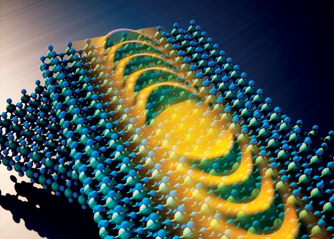
In systems formed by layers of two-dimensional materials, such as two or more graphene sheets, a slight rotation of around 1.1 degrees can produce radical changes in the properties of the structures, especially electronic properties, and can result in superconductivity. Misaligning one of the overlaid graphene sheets generates images within an interference pattern known in physics, mathematics, and the visual arts as a moiré pattern, marked by light and dark fringes, as shown in the illustration of graphene sheets on the first page of this article. When printing graphics, a colored figure is generated by perfectly overlapping four differently colored layers (black, yellow, cyan, and magenta). If one of these layers is twisted a little in relation to the others, the image is out of sync and a moiré pattern is created. But something seen as an error in the arts can be seen as a success or at least a fascinating field of study in twistronics.
Advanced Science Research Center / CUNY
The properties of other 2D materials, such as the molybdenum trioxide sheets shown in the drawing to the right, are also altered by rotating one layerAdvanced Science Research Center / CUNYPerfectly misaligning one of the graphene sheets to change the material’s properties is not a simple task. “This is one of the most difficult parts of our work,” says physicist Andreij Gadelha, lead author of the Nature article, who completed his doctorate at UFMG in 2019. Determing the magic angle requires a certain level of manual dexterity. The researchers use optical controls that literally need a human hand to achieve the desired displacement angle. “It took me a year to master the technique,” says Gadelha. However, systems composed of layers of two-dimensional materials sometimes spontaneously reverse the small rotation and perfectly re-juxtapose themselves, putting an end to the magic angle.
There is still no consensus on why displacing one of the layers of a two-dimensional structure changes the material’s characteristics. In the case of superconductivity, it is speculated that the interactions between electrons and internal vibration modes associated with quantum phenomena, which are still not fully understood, change significantly as a result of architectural changes between the layers of two-dimensional materials. “One of the explanations for the effects of twistronics is the theory of electronic correlation,” explains physicist Rodrigo Capaz of the Federal University of Rio de Janeiro (UFRJ), who since last October has been working temporarily at the Brazilian Center for Research in Energy and Materials (CNPEM) in Campinas, funded by a FAPESP scholarship for visiting researchers. “According to this concept, the electrons in the sample stop behaving individually and start to act as a collective unit.” Capaz has already published articles describing simulations of up to four graphene sheets on top of each other, of which two are rotated.
The nanoscope is like a more powerful, higher resolution version of a Raman spectrometer integrated with a scanning probe microscope, used to generate images at an atomic level. It can “see” structures as small as 10 nanometers, covering anything from 50 to 70 carbon atoms, depending on the molecule and its phase (state of matter). “Our device is 10 to 100 times more efficient than other commercial equipment available on the market,” says Jório. Raman spectroscopy is a non-destructive technique that uses light to analyze the physical and chemical properties of a compound based on interactions between the light and the molecular vibrations of a material.
Put simply, the technique works as follows: a sample is illuminated by a laser, and the way the light scatters on the object of study is observed. Most of the scattered radiation will have the same frequency as the light emitted. A small portion, however, will display different wavelengths (colors). Based on the characteristics of this specific scattered light, it is possible to infer certain properties of the material, such as its structure, phase, and molecular interactions. Indian physicist Chandrasekhara Venkata Raman (1888–1970) won the Nobel Prize in Physics in 1930 for discovering this light scattering effect (hence the name of the method).
The nanoscope functions by directing light over a circular area with a diameter of about 1 micrometer, equivalent to a thousand nanometers. Then, using a nanoantenna with a tip that is 10 nanometers in diameter, the device scans an area 100 times smaller than the one initially illuminated. This sweep of the sample’s surface is used to record Van der Waals forces, a type of weak interaction between atoms and molecules and the locally scattered light, allowing the equipment to reconstruct an image of the material based on these measurements. The technique’s maximum resolution is determined by the size of the nanoantenna’s tip. The nanoantenna, which is pyramid shaped and was developed by UFMG and INMETRO, is the devices unique selling point. Without it, it would not be able to achieve the same high resolution. Due to the physical limitations of light diffraction, the maximum resolution of conventional optical microscopes is around 500 nanometers.
Discovered in 2004 by Andre Geim and Konstantin Novoselov, a pair of Russian physicists from the University of Manchester, UK, who would later win the 2010 Nobel Prize for their achievement, graphene is one of the world’s simplest and most surprising materials. It is simultaneously light, flexible, and extremely resistant, mechanically speaking. It is also a good thermal and electrical conductor. Unexpected properties have already been verified experimentally in different forms of graphene, both pure and combined with other chemical elements or compounds. In twistronics, the most notable aspect of graphene sheets and other two-dimensional materials that can be stacked and rotated is that there is no need for chemical changes to achieve surprising results, such as superconductivity. Simply rotating one of the layers at the correct angle seems to be enough.
The foundations of what would become twistronics stem from the second half of the previous decade. In 2007, Brazilian theoretical physicist Antônio Castro Neto, now working at the National University of Singapore, suggested that compressing two slightly misaligned sheets of graphene could result in new electronic properties. In 2011, Allan MacDonald, from the University of Texas, USA, proposed that significant electronic changes could occur in two graphene sheets if one of them were rotated by about 1.1 degrees—the magic angle. The field grew slowly until seven years later, one of MacDonald’s graduate students, Spaniard Pablo Jarillo-Herrero, observed superconductivity in experiments with graphene sheets rotated by the magic angle.
“Jarillo-Herrero’s research gave the field a new lease of life,” says theoretical physicist Dario Bahamon, from the Center for Advanced Research in Graphene, Nanomaterials, and Nanotechnologies (MackGraphe) at Mackenzie Presbyterian University in São Paulo, funded by FAPESP. This year, Bahamon and his colleagues from the Autonomous University of Madrid published a paper on stacked graphene sheets, one of which was rotated by the magic angle. “We simulated the magnetic response to this situation.” If, in addition to sparking interest among theorists, experimental physicists continue studying rotated graphene sheets in their labs, it is possible that a small market for these nanoscopes could emerge. That is what Ado Jório and his colleagues at UFMG are hoping for. “I received lots of invitations to conferences after the article was published in Nature. There is great interest in learning more about the device,” says Jório.
Project
Atomic resolution in atomic force microscopy (no. 20/06257-7); Grant Mechanism Research Grant – Visiting Researcher – Brazil; Principal Investigator Adalberto Fazio (CNPEM); Grant Beneficiary Rodrigo Capaz (UFRJ); Investment R$194,320.
Scientific articles
GADELHA, A. C. et al. Localization of lattice dynamics in low-angle twisted bilayer graphene. Nature. Vol. 59. Feb. 18, 2021.
CAO, Y. et al. Unconventional superconductivity in magic-angle graphene superlattices. Nature. Vol. 556. Apr. 5, 2018.