The next two years should see Brazil’s first production of new-generation semiconductor modules for use in smartphones and Internet of Things (IoT) devices, if plans pan out. US-based Qualcomm, the world’s fifth-largest semiconductor firm, announced in February it plans to build a facility to produce its new QSiP (Qualcomm System in-Package) technology in Campinas, São Paulo State. The next-generation modules will be produced by a joint venture with Taiwanese semiconductor manufacturer USI, a subsidiary of ASE Group, one of the world’s largest chip assembly firms.
“We decided to produce a chipset product in Brazil that is not being made anywhere else in the world, rather than setting up a facility to produce integrated circuits that are already being produced in Asia,” says Rafael Steinhauser, president of Qualcomm Latin America. “Brazil will be one of the first countries to deploy this technology.” The new Qualcomm product is a module comprising about 400 elements, including memory, processor, connectivity, and communications systems. “Some of the key advantages of QSiP technology include simplified smartphone design, faster time to market, and a smaller footprint [in mobile phones] that allows manufacturers to design devices as slim as 6 millimeters (mm) while using larger batteries,” explains Steinhauser.

Eduardo Cesar
A prototype of the module to be produced in Brazil by Qualcomm and USIEduardo CesarDuring a visit to the University of Campinas (UNICAMP) last month to speak at an inaugural lecture at the School of Electrical and Computer Engineering (FEEC), where he earned his degree, Qualcomm President Cristiano Amon explained that his side would be the technology partner while USI would handle assembly and plant management proper. Site selection is expected to occur later this year and some activities, such as component testing for other USI units, will be initiated ahead of assembly line completion. “We want the first smartphones with this technology to be on the market by the end of this year,” Amon said. This will require QSiP modules to be initially imported from China.
The new joint venture is expected to create around 800, mostly high-skilled jobs and will involve investments of US$200 million (R$660 million) over a period of five years. To locate in Brazil, the two firms have been offered a lower tax on sales and services (ICMS) rate as well as tax incentives linked to Processo Produtivo Básico (PPB), a federal program that awards benefits to companies locating parts of their manufacturing lines in the country.
The announcement of the new plant has injected new life into Brazil’s microelectronics industry, years after an unsuccessful foray into the competitive global semiconductor market a few decades ago. “Obviously, we’re lagging far behind in this industry. The sector began to languish in the 1990s when the Fernando Collor de Mello administration abolished Brazil’s protectionist policy. And while still very incipient, it is now beginning to thrive in terms of revenues, number of players, and available technologies,” says electronic engineer Rogério Nunes, president of the Brazilian Semiconductor Industry Association (ABISEMI). “I’m delighted that the Qualcomm-USI joint venture will be locating here and producing a product that is innovative at a global level.”

Nabor Goulart / Agência Freelancer
CEITEC technicians during the fabrication stageNabor Goulart / Agência FreelancerNunes believes Brazil needs to claim its share in the semiconductor industry, which generated global revenues of US$419 billion last year. ABISEMI estimates that its 11 members—four chip design firms and seven integrated circuit packaging operations—generate about US$1.5 billion in annual revenues, accounting for only 0.36% of global sales. “It’s too little. With Brazil holding a slice of about 3.5% of the global information technology [IT] market, in theory we could boost semiconductor revenues by about 10 times just by serving the local marketplace,” Nunes says.
Trade deficit
According to experts, Brazil’s limited presence in this segment carries a high cost. The country imports about US$3.6 billion annually in semiconductors, and in 2017 the balance of trade in the electronics industry was negative by US$23.8 billion. “Not only does it create a large deficit for the country, but the lack of world-class semiconductor capabilities makes Brazil technologically vulnerable,” says physicist Luís Fernandez Lopez, head of the Academic Network at São Paulo (ANSP), which provides internet access to education and research institutions in São Paulo. “IT is among the fastest-growing industries globally, and chips are its staple product. So it’s critical that we build expertise in designing, building, and manufacturing integrated circuits.”
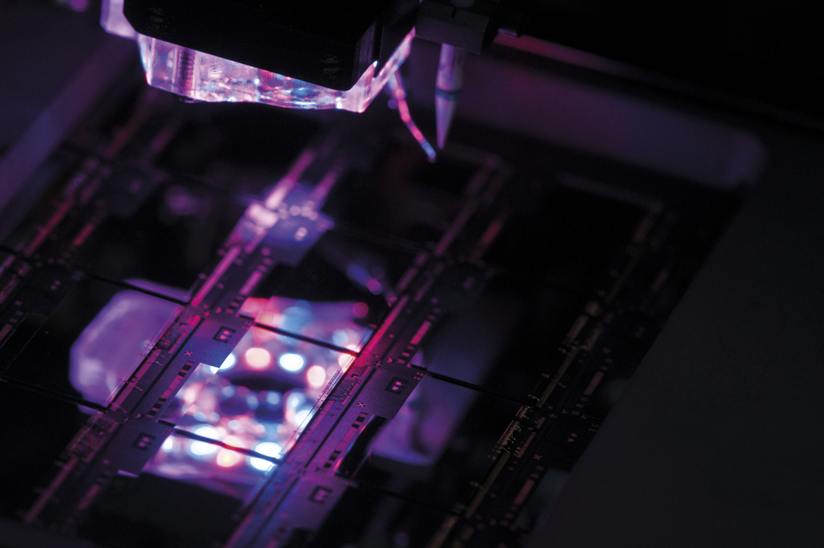
Léo Ramos Chaves
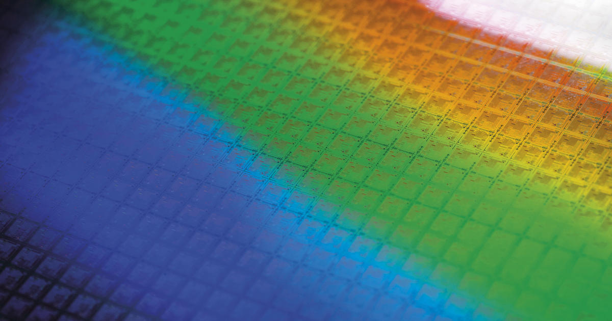
The final stage of integrated circuit production at the Eldorado Research Institute labLéo Ramos ChavesThe semiconductor value chain has three links: schematics and printed circuit designs are developed at design houses; wafers—the ultra-thin, high-purity silicon disks, up to 300 mm in diameter, from which chips are made—are manufactured at facilities known as foundries; final product assembly, which includes packaging (in which chips are encapsulated in protective cases providing a secure connection to printed circuit boards) and testing, is done at packaging firms—Qualcomm’s new facility falls within this category (see infographic).
“An international study commissioned by the Brazilian Development Bank (BNDES) in the early 2000s revealed the importance of Brazil gaining a foothold in the semiconductor value chain to increase technology density and job quality,” says Maurício Neves, head of planning at BNDES. “The survey showed that funding was needed for investment at all levels of the ecosystem—from design houses through foundries to packaging. And BNDES responded.” Neves notes that nowhere in the world have countries succeeded to develop a strong semiconductor industry without active, long-term government support.
According to electrical engineer Jacobus Swart, a professor at FEEC-UNICAMP, BNDES efforts have had some results. “Brazil is doing well in terms of design houses and packaging firms, but we are still far from having wafer foundry capabilities. Two companies created in recent years to develop these capabilities, state-owned CEITEC and private-owned Unitec, are still struggling,” says Swart. “These firms have already received a significant amount of funding from BNDES and the Brazilian Funding Authority for Studies and Projects (FINEP), through both equity and debt finance, but neither has launched into wafer production yet.”

The Federal Government created CEITEC in 2008 to become Brazil’s first integrated device manufacturer (see Pesquisa Fapesp issue no. 137). Ten years later, this is yet to be achieved. “In general, new chips are designed in Brazil, wafer fabrication is done offshore, and final production—including packaging in some cases—is completed at CEITEC,” explains mechanical engineer Paulo de Tarso Mendes Luna, CEITEC’s CEO.
Located in Porto Alegre, the plant has the technology to produce 600-nanometer (nm), or low-density, chips. “For smaller chips, part of the process is offshored,” Luna explains—the modules Qualcomm plans to produce in Brazil are high density. “Chip density denotes the level of miniaturization. The smaller the figure, the larger the number of transistors and the wider the functionality. Computers and mobile devices typically incorporate high-density chips,” explains Swart of UNICAMP. He notes, however, that there is still a market in Brazil for less complex integrated circuits like the ones CEITEC produces. “Simpler, lower-cost technologies can be produced with this level of miniaturization. Only a handful of companies worldwide produce high-density semiconductors.”

With a capacity to produce about 20 million chips per month, CEITEC has a portfolio of seven integrated circuits designed for livestock, people, and vehicle identification, inventory management, asset tracking, and other applications. The government has injected around R$800 million into the business. “That’s less than what is typically invested to develop manufacturing operations in this industry, which is usually to the tune of more than US$1 billion,” says Luna. The company has reported cumulative losses of R$40 million, but expects to move into profit by 2021. “The semiconductor industry usually takes 10 to 15 years to break even.”
Wafer foundry
Another initially ambitious, but still incipient, venture is Unitec Semicondutores. Founded in 2012 in Ribeirão das Neves, on the outskirts of Belo Horizonte, Minas Gerais State, the company was part of the conglomerate created by one-time billionaire Eike Batista and previously traded as SIX Semicondutores. In 2014, when Batista’s companies began to flounder, his stake in the venture (33%) was sold to Argentine group Corporación América, which operates airports in Brasília and Natal.
“Unitec was meant to operate across the entire value chain, from chip design to application in smart solutions. Currently our operations are limited to design and packaging,” says CEO Frederico Blumenschein. The plant is still only partially operational, despite investments to date amounting to around R$1 billion, with R$245 million coming from BNDES through equity finance for a 33% stake in the business. Unitec expects to secure further investment to complete the fabrication plant.

When fully operational, Unitec will have the capacity to manufacture up to 130,000 wafers per year—each producing thousands of chips. The plant will specialize in 90 nm and 130 nm integrated circuits with CMOS (Complementary Metal Oxide Semiconductor) technology licensed from IBM, IT multinational which has an 18.8% interest in the company.
“CMOS technology, the backbone of modern digital circuits, is most commonly used in microprocessors, memory, and radio frequency communication blocks” explains Blumenschein. The company currently has two chip designs, one for logistics tracking and the other for street lighting applications. “The prototypes have been successfully tested. They might initially be produced with support from partners pending completion of the plant in Ribeirão das Neves.”

Eduardo Rocha / RR Foto
A Unitec employee encapsulating radio frequency identification tagsEduardo Rocha / RR FotoAccording to Ricardo Rivera, head of Information and Communication Technology (ICT) Industries at BNDES, Unitec was not intended to be a pure-play foundry business like the established players in Asia, producing chips for the computer and mobile device market at large scale. “Unitec uses a hybrid model—a fabless firm with foundry capabilities. From a market positioning standpoint, its success will hinge on having the design capabilities to develop chips suited for a wide variety of segments, from IoT to automotive and life sciences,” he says. And, he continues, because it uses non-state-of-the-art process technology, it needs to develop a product mix that is not entirely a low value-added offering. Fabless companies design and market chips under their own brand and manage the overall business lifecycle, but rely on outsourced manufacturing capabilities, which they lack. This is the model that Qualcomm operations typically fall under.
Although a fully operational foundry still remains on the distant horizon, Brazil already has a network of design houses and packaging firms at varying levels of maturity. In the first group are names such as the Eldorado Research Institute in Campinas, a nonprofit organization that is a leading player in IT research and development. “We specialize in leading-edge integrated circuit design. We have 60 designers, most of whom were trained within the CI Brasil program,” says electrical engineer José Eduardo Bertuzzo, executive manager for Technology at Eldorado.
CI Brasil was a Federal Government initiative launched in 2005 that aimed to bring industry and academia together to create a microelectronics ecosystem that would usher Brazil onto the global semiconductor market stage. One of its goals was to train an expanded pool of chip design experts. “The program trained more than 800 designers and led to the creation of around two dozen design houses,” says Bertuzzo. “Integrated circuit design is a field where we can excel, as we have some very talented designers in Brazil.”
CI Brasil has trained more than 800 chip designers and supported the development of design houses
A state-of-the-art laboratory
At year-end 2017, Eldorado opened a chip prototyping laboratory built under a technological cooperation agreement with Smart Modular Technologies of Atibaia, São Paulo, a leading packaging firm specializing in memory products for computers and mobile devices. Equipped with clean rooms (superfiltered environments with a minimal number of particles per cubic meter) such as those used in chip fabrication and testing, the laboratory is being used to develop new semiconductor technologies and for training.
The facility has been developed as part of the Semiconductor Industry Development Program (PADIS), another Federal Government initiative in support of the domestic chip industry. Smart Modular Technologies, based out of Newark, New Jersey, has operations in eight countries. Its Brazilian site is the only facility with dicing, packaging, and testing capabilities using domestic technology. Its flagship product is an advanced smartphone memory module technology called eMCP (Embedded Multimedia Chip Package).
Tecnosinos, a technology park located on the Vale do Rio dos Sinos University (UNISINOS) campus, about 35 kilometers from Porto Alegre, is home to another packaging and testing firm. HT Micron—a joint venture of Brazilian Parit Participações and South Korean Hana Micron—was created in 2009 with support from the Brazilian government (via BNDES and FINEP) and the ambition to become one of the largest players in the sector. The plant started operations in 2014 and was expected to produce 360 million chips per year within two or three years’ time, but has yet to deliver.
The company, which did not respond to requests for interviews, said in a statement on its website that “R$110 million have already been invested in the project, and further investment of R$260 million is planned over the coming years.” In early 2017, HT Micron’s operational woes led to electrical engineer Ricardo Felizzola stepping down after six years as CEO, with South Korean Chris Ryu now filling his role.
Luís Fernandes Lopez of ANSP Network believes the setbacks that most semiconductor ventures in Brazil have run into in recent years stem to a great extent from a lack of government policy. “As a basic industry, the semiconductor sector takes years to build momentum. It requires coordinated policy support in these nascent years, with medium- and long-term funding commitments and with firms working toward set goals, or it will struggle to flourish,” says Lopez. “We will otherwise continue to lag in a sector as vital as semiconductors.”
Republish