Chicago-based RHK Technology, a company specializing in atomic-resolution scanning tunneling microscopes, unveiled a newly developed product with an optimized light-collection system during the American Physical Society conference held in March this year in the US. The device collects light into the microscope with more than three-times-higher efficiency than previous models. The new system was developed at the Gleb Wataghin Institute of Physics at the University of Campinas (IFGW-UNICAMP), in Brazil.
The project was led by physicist Luiz Fernando Zagonel, a professor at IFGW, in collaboration with Ricardo Javier Peña Román and Yves Maia Auad, both doctoral researchers at respectively UNICAMP and Paris-Saclay University, in France. For their new technology, now licensed as part of a market-ready product, the team received a 2022 Inventors’ Award from UNICAMP in the “Technology Uptake” category.
“This new technology provides a crucial capability for some of our customers: the ability to study light emission from samples and their electronic and topographic characteristics,” RHK Technology founder and CEO Adam Kollin told Pesquisa FAPESP. “The system can be incorporated into one of our products with minor modifications, making it easy to deliver these new capabilities to the scientific community.” The new device has been branded as PanScan Lumin-SLT.
The project, funded by FAPESP via its Young Investigator Program, was created to address a need Zagonel identified during a postdoctoral fellowship at Paris-Sud University (now Paris-Saclay University) between 2008 and 2010. He was researching semiconducting nanowires and was unable to find a microscope that met his research requirements. After contacting different suppliers, he was offered equipment that captured only a fraction of the light emitted by the sample—between 2% and 5%. He was left dissatisfied as a customer and frustrated as a researcher.
Léo Ramos Chaves / Pesquisa FAPESPIFGW-UNICAMP’s scanning tunneling microscopeLéo Ramos Chaves / Pesquisa FAPESP
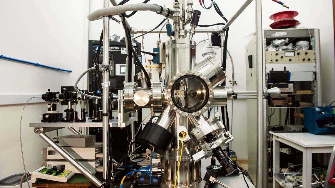
So he turned his need into a technological challenge. “During the two years I spent in France, I was able to identify and resolve several research problems. This turned into multiple research papers and patents,” says Zagonel. Back in Brazil in 2015, his FAPESP-funded research project led to the development of a device with a light-capture efficiency of up to 72%. The system has three components: a small optical table designed to be attached to a scanning tunnelling microscope; a manipulator system with movement in three directions; and a parabolic mirror.
Understanding the significance of these improvements requires an understanding of how scanning tunnelling microscopes (STM) work. To obtain images with atomic resolution, these devices exploit a quantum phenomenon known as tunneling current, which occurs when electrons move in between two surfaces a distance of approximately 1 nm—or a billionth of a meter—apart. In scanning tunnelling microscopy, electrons pass between the microscope’s metal tip and the sample, resulting in energy transfer to the sample, which emits light that is then captured by the microscope.
“The problem was being able to capture the emitted light using an STM operating within an ultrahigh vacuum environment and at low temperatures, which is what the device was designed for,” explains Zagonel. To illustrate the challenge, the researcher makes the following analogy. “Imagine a car’s headlight. It has a light source and a reflector designed to collect most of the emitted light and point it forward to the road. Without the reflector, much of the light would be emitted in every direction rather than toward the road. The same principle applies to an STM microscope. There is a tiny light source, which is the sample itself. We needed to find a way to capture as much of the light as possible and direct it forward so it can be measured.”
Most of the equipment then available on the market, says Zagonel, used optical fibers or lenses that captured only a small fraction of the light emitted by the sample. The device developed at UNICAMP uses a miniaturized parabolic reflector to solve this problem. The improved light collection efficiency helps to produce more detailed data about the light emitted by the specimen, providing a wealth of data about materials with scientific and commercial applications, such as semiconductors, metal nanostructures, and other nanostructured materials.
“We developed a novel technological solution. Conventional fiber-optic-based systems have a very low efficiency, not exceeding 5%. Using lenses, this can be improved to between 10% and 20%, which is still too little. Getting past the 50% barrier would require the use of parabolic or ellipsoid reflectors. This improves light collection efficiency, but aligning the mirror remained a challenging problem,” explains Zagonel. “Our solution combines a parabolic reflector with a three-axis, high-precision manipulator. This assembly allows us to align the mirrors so the system actually works.”
Now, with additional FAPESP grant funding, Zagonel is using his invention to research materials that can potentially be used to create light-emitting diodes and solar cells made of inorganic perovskites (see Pesquisa FAPESP issue nº 260). “There are a number of problems related to renewable energy that need to be resolved,” says Zagonel. “And our equipment can help achieve a better structural understanding of materials that could be key to developing new renewables technologies.”
From patent to shelf
This was UNICAMP’s first licensing agreement giving it 100% ownership of patent rights as the licensor. “Under previous agreements we always co-owned the patent rights with a partner company,” explains Iara Silva Ferreira, who serves as partnership director at UNICAMP’s innovation agency, INOVA. The time from patent to market was surprisingly short. UNICAMP applied for a patent on the invention in July 2020, and by December 2021 it had signed a technology transfer agreement with RHK.
Two factors were crucial in speeding up the process: the researcher had prospected for commercial partners early in the project, and the technology had reached a high level of maturity, explains Ferreira. “Professor Zagonel identified an unmet demand in the market, and did more than just apply for a patent. And the solution’s Technology Readiness Level (TRL) helped to shorten time to market.”
According to Ferreira, whereas most of the University’s projects never went past a TRL of 3—on a scale of 1 to 9—the device developed at IFGW was at a TRL of 5, meaning it could be readily integrated into RHK’s product. The higher the TRL, the readier the technology is for the market.

Léo Ramos Chaves / Pesquisa FAPESPThe rear window of the chamber used to allow the passage of light for measurementLéo Ramos Chaves / Pesquisa FAPESP
“Our invention’s higher TRL was partly because, from very early in the project, we had a company interested in later licensing the technology,” says Zagonel. “In addition, our solution incorporates important features, such as alignment protocols, and had been previously tested and proven by journals.”
Zagonel notes that as he was developing the device he approached a number of manufacturers as potential partners. RHK was especially receptive to his ideas and agreed to sell a microscope specially adapted for his invention to the Photovoltaics Research Group in IFGW’s Applied Physics Department. The equipment, newly added to FAPESP’s inventory of shared equipment, is now available to other research groups.
“When our project proved successful and we started publishing our first papers, we soon began discussing a potential technology transfer. INOVA has provided assistance and intermediation support at each step in the process, from our early results to now,” says Zagonel.
“Support from an innovation agency can be crucial in bringing technology developed in an academic setting to the market,” says Luciana Hashiba, a researcher at the Center for Innovation at the Getulio Vargas Foundation’s School of Business Administration in São Paulo (FGV/EAESP). “And having a technological innovation group at a research institute can help researchers develop the project with a market-oriented mindset,” adds Hashiba, who also serves as assistant coordinator of FAPESP’s Scientific Board. “This can make all the difference when it comes to technology transfer.”
RHK is now planning to launch initiatives to boost sales of their new system. “As soon as we finish the marketing literature, we will start an advertising push for the microscope,” says RHK CEO Kollin. “We also plan to organize a technical webinar with professor Zagonel to provide a sound scientific explanation of the new system.”
Projects
1. Heterostructures in semiconducting nanowires: nanometric light emitters studied by scanning tunneling microscopy (nº 14/23399-9); Grant Mechanism Young Investigator Award; Principal Investigator Luiz Fernando Zagonel (UNICAMP); Investment R$617,335.61.
2. Optically active materials studied by scanning tunneling microscopy (nº 21/06893-3); Grant Mechanism Young Investigator Award; Principal Investigator Luiz Fernando Zagonel (UNICAMP); Investment R$1,010,676.95.
Republish
