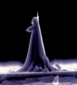
DANIEL UGARTE / UNICAMPAt the tip of the tip: nanotube welded to a siliconDANIEL UGARTE / UNICAMP
For several months, Denise Nakabayashi and Alberto Moreau spent several hours a day handling a joystick – similar to that used for video games – in a small room at LNLS, the National Laboratory of Synchroton Light in Campinas. Anybody watching them might think that they were playing. But they were not. The joystick was connected to a metal cube that was slightly smaller than a shoebox, enabling them to control two tiny bars used to manipulate a cylinder made out of several thousand carbon atoms. The objective was to fix this tube – called a carbon nanotube because of its tiny nanometric diameter – to the tip of a silicon cone, hundreds of times bigger, thus greatly increasing the resolution of an atomic microscope. This equipment enables one to produce three-dimensional images of the matter on a nanometric scale (millionths of a millimeter) and also to manipulate atoms and molecules, as it maps the surface in a way similar to a person using their finger to read Braille. The smaller the tip’s diameter, the more details it detects.
Many attempts were necessary – each took five to six hours of work – before success was achieved. Denise and Alberto would place the nanotube at a close distance, and it would promptly adhere to the silicon cone, attracted by the Van de Waals electric forces, observed only on the scale of atoms and molecules. But this did not work out. Extremely flexible, the nanotube would bend easily if by chance they placed it against the surface to be mapped. Even in the inside of a vacuum camera, the nanotube would start vibrating as a result of thermal energy, like string waving in the air, and could stretch to a length of more than one thousand nanometers.
At other times, this apparently delicate tube – which is as resistant to tension as silk or a spider’s web – would separate from the silicon cone. So Denise and Alberto decided to weld it to the cone, using the microscope’s electron beam. Pointing towards the region where the nanotube touches the silicon cone, this beam accumulated the carbon atoms dispersed in the vacuum – there are always some impurities that remain in lab-created vacuums – at the point of contact. But the result was not always satisfactory. “The nanotube still vibrated and sometimes would come undone,” says Denise.
The solution was to improve the welding. Denise and Alberto increased the welding time from 20 to 60 minutes. When they looked at the tip again, they noticed that a crust had formed around the nanotube. They solved two problems at the same time: they fixed the nanotube and eliminated the unwanted vibration. “The result was similar to that obtained with concrete in construction; this concrete is flexible and resistant,” says physicist Daniel Ugarte, Denise’s project advisor, who developed nanometric instruments at the LNLS and at the State University of Campinas (Unicamp).
After preparing the three tips, Alberto, who is working on his doctorate in physics under physicist Monica Cotta, at Unicamp, used them to produce images on the surfaces of semiconductor materials. To everyone’s astonishment, the same tip produced more than 400 images, without becoming damaged in any way or losing its resolution. This kind of durability is at least 20 times higher than that of the tips of commercially available atomic microscopes made of silicon, which break after 10 or 20 images. “The silicon tips are fragile and break if they accidentally touch the analyzed surface. The tips of the nanotubes, however, are flexible, bending and returning to their original position,” says Monica, who is now beginning to use this equipment to study biological systems, such as the Xylella fastidiosa bacteria and the biofilm that forms inside orange tree vases. “The reinforced nanotube tips don’t damage the cells,” says Monica.
Because they did not quite understand why the carbon-welded tip of the nanotube became more stable, Monica, Alberto, Ugarte and Denise had to ask theoretical physicists for help. They contacted Douglas Galvão and Vitor Coluci, also from Unicamp, who use computer programs to try to understand what happens at the atom level. In various simulations, they noted that the extra layer of carbon around the nanotube absorbs the impact of the shock against the obstacles, as described by researchers in an article to be published in Nano Letters. As a result, the reinforced tip is more stable – and produces images with a much better definition – than the tips that other teams had built only with nanotubes.
If the result is so good, wouldn’t it be worthwhile to patent the production method? Not in Ugarte’s opinion. “The market for these objects is limited and the investment to produce them on a larger scale is enormous,” he says. Moreover, he adds, if they obtain tips that increase the resolution of those microscopes even more, it would be more advantageous for them to use the tips in their own research studies. “In this way,” says Ugarte, “we would enjoy an advantage for a while.”
Republish